The transistor common base configuration is just as simple as the other two (common collector, common emitter) configurations, but far less known and used – which is a regrettable mistake, because it is absolutely awesome and has little-known characteristics which we’ll look into right away!

Operating principle
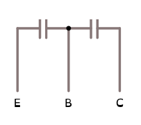
At first look, the common base configuration seems “impossible” (ground at the base???) and even if it worked, the benefits wouldn’t be obvious. The base configuration circuit diagram above is the most commonly shown. It suggests that some voltage will be applied to the transistor emitter which should cause a voltage change at the collector output. But since the base is grounded the transistor will never conduct and hence the collector voltage will never change. So how does this circuit work?
What most of these simple diagrams don’t tell you is that they actually assume that the “input” voltage drops below 0V so that the potential difference between base and emitter becomes positive and the transistor conducts current which causes a voltage drop at “output” (collector). Since negative voltages aren’t practical, all we need to do is “lift” the base voltage higher than the input signal.
Assuming an input signal between 0V and 1V, the simplest working configuration consists of biasing the transistor base to a voltage higher than the input signal voltage.

In the diagram above the input signal (green) is a sine wave with 0,5V amplitude and creates an almost rectangular output signal (red) between 0V and 5V with pretty steep slopes.
What is there to be learned about the common base configuration from this experiment?
- It has steep amplification characteristics
- It amplifies voltage (a lot)
- It doesn’t change the phase (unlike ie. common emitter configuration)
For an amplifier, the resistor values are rather low and the power consumption is probably high. Let’s try this again, with a few changes. We’re going to bias the base with a low-impedance voltage source (0,8V) and a larger resistor (10KΩ) at the collector. There’s also a small resistor between emitter and input signal just to limit the maximum current through the transistor.

The output signal has again a rectangular shape with even steeper slopes; so increasing the collector resistor increases amplification. The 0,8V at the base and the very low resistor at the emitter (1Ω) are worth a closer look. This configuration potentially creates a large current which could destroy the transistor, so clearly this isn’t a real-world circuit, but it hints at another characteristic of the common base configuration: is has a low input impedance. So let’s summarise what we know so far about the common base configuration:
- It has steep amplification characteristics
- It amplifies voltage (a lot)
- It doesn’t change the phase
- It has a low input impedance
- It has a high output impedance
Applications
Wikipedia mentions three fields of application: high frequency amplification, digital circuits and low impedance amplification such as in microphones.
The common base configuration has a low input capacitance and isn’t affected much by the Miller effect which caps high frequencies. The easiest way to understand the Miller effect is to imagine the NPN (or PNP) transistor as a semiconductor sandwich stacked with three layers.

In a way, this looks like two capacitors in series with the collector, base and emitter bridged by those capacitors. While low, the transistor’s own capacitance will attenuate high frequencies, reduce amplification and increase leaking. Common base configuration doesn’t suffer from this effect so much because the base-emitter current is already high while the base-emitter voltage is low: there isn’t much potential difference left to bridge for the intrinsic capacitance.
The next application is digital circuits, if the steep amplification slopes didn’t give this application already away. The utility in discrete circuits is kind-of obvious; the clear separation between “high” and “low” voltage levels, the low power requirements for driving the output signal and the low input capacitance (see Miller effect) make the common base configuration an interesting choice for fast switching digital circuits.
The last application is circuits where a low input impedance is required. Counter-intuitively, this is a great use-case for buffer circuits. A buffer circuit is meant to feed the output signal of one circuit to the input of another circuit without drawing much power from the first circuit. A classic example is the power amplification of an LC oscillator which produces a weak sine signal. We want to grab that sine and amplify its power, eg. because we want to send it into an antenna.

If we connect the antenna directly to the oscillator (the wavy circle on the left), then signals the antenna catches from the environment (there is plenty of EM radiation around) will disturb the oscillator leading to a dirty signal. Even if we directly connect the power stage (the transistor at the right of the diagram) directly to the oscillator, it will draw too much power from the oscillator and dampen its oscillation. The buffer (the transistor in the middle of the diagram) has a high input impedance (1MΩ), draws very little power from the oscillator and thus doesn’t interfere with it.
But low interference can be achieved not only with high input impedance (drawing little power), but also with low input impedance when used correctly. The trick here is to make the buffer a part of the input circuit (eg. the oscillator). Since the buffer has a low impedance, it would look just like a connecting wire with a slightly higher resistance.

The input signal in this configuration is a sine wave that oscillates between -0,5V and +0,5V and is coupled through a transformer to a common base configuration. The base is biased in such a way that the collector (output) rests at 2,5V (half the operating voltage). This configuration interferes very little with the input signal; the transformer can have an almost arbitrarily low impedance. As the common base configuration is driven by input current and not input voltage, the transformer can be a step down transformer which creates very little load on the oscillator. By making the transformer part of the input circuit (eg. the transformer replaces the coil in the LC part), it can replace a wire in the input circuit and drive all its current through that transformer.
Wikipedia mentions that the configuration combo of transformer and common base is used with microphones which seems to make sense, as the circuit doesn’t draw any power from the oscillating membrane and thus doesn’t impede its movement.
