1-Transistor feedback amplifier

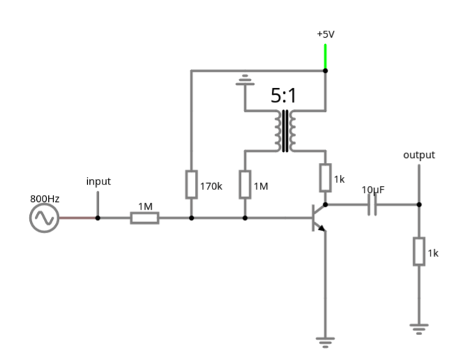
Many old AM receiver circuits use positive feedback (routing some of the already amplified output signal back into the amplifier's input) for more gain. These circuits (eg. the reflex receiver [REF]) are fascinating designs which, although not overly complex, aren't easily understood. Starting with an existing circuit design, I tried to isolate the feedback loop … Continue reading 1-Transistor feedback amplifier

An even better switching amplifier

From the producer of A switching amplifier [AM1], A better switching amplifier [AM2] comes part 3: An even better switching amplifier. A quick recap: we're looking into class D switching amplifiers for their high efficiency and power output. The first amplifier sampled the input signal by taking voltage snapshots with a capacitor and measuring the … Continue reading An even better switching amplifier

Comparing the efficiency of DC voltage boost circuits

Overview & disclaimers This post compares the power efficiency of some voltage boosting circuits. The circuits discussed here are: Buck converter Parallel buck converter Serial buck converter Pulsed transformer Joule thief Honorary mentions What we're doing here is neither complete nor scientific and aspires to more than it delivers. Comparison base line The generic version … Continue reading Comparing the efficiency of DC voltage boost circuits

Simplified double push-pull amplifier

There exists a simpler design for the double push-pull amplifier with cross-over compensation [DPP]. A quick recap of the previous design: the input signal is divided into a reference phase and an inverted phase, each phases are amplified separately and drive two push-pull amplifiers [PPA] respectively. What happened so far: while in absolute terms simple, … Continue reading Simplified double push-pull amplifier

帶交叉補償的單推挽放大器

親愛的讀者! 這個實驗是我原帖的(自動)翻譯成中文。 原帖標題為“帶交叉補償的單推挽放大器”。 我希望文本在你的語言中是有意義的,我希望你喜歡閱讀。 這將是一個快速的。具有交叉補償的雙推挽放大器解釋了一種高功率放大器電路,它創建一個平衡點併校正交叉。一個更簡單的電路版本依賴於兩個相等的電壓源來創建 0V 平衡點,因此它使用單個推挽對而不是兩個。此外,由於我們不再需要 180° 反相信號,因此單個差分放大器足以校正交叉。請注意,雖然電路會放大功率(通過放大電流),但它不會放大電壓:2V 輸入信號將導致 2V 輸出信號。 關於電路圖的一些簡短說明: 40Hz AC 是一個任意輸入信號,但它應該在 0V 左右平衡 - 一個不平衡的信號(例如,如果它在幅度的 + 側花費更多時間而不是在 - 側花費更多時間)會導致通過 PA 晶體管和負載的淨直流電流,這可能會使電路的某些部分過載,或者至少需要更多的冷卻。 4Ω 電阻器是任意輸出負載(如揚聲器或變壓器線圈)的佔位符——這就是人們首先要構建此放大器的原因。 兩個電池必須具有相同的電壓、內阻和功率,以便即使在負載下,它們也能準確地平衡在 0V(接地)。它們的電壓取決於電路的其餘部分,我認為 5-12V 對於大多數應用來說應該沒問題。 晶體管是一對 PNP 和 NPN MOSFET,其規格應足以處理計劃的負載。它們的閾值電壓不應太高,但理論上是無關緊要的,因為運算放大器負責處理任何交叉失真。 差分放大器有多種用途:1. 它通過其高輸入阻抗將輸入信號從放大器中解耦。2. 它放大輸入信號3. 它通過比較輸入信號和輸出信號來補償輸出中的交叉失真4. 它可以在一定範圍內補償不平衡的電壓源 由於電路不放大電壓,因此運算放大器的標稱輸出信號幅度應該足夠大以驅動 MOSFET 晶體管對。特別是對於高頻,運算放大器通過提供足夠大的輸出信號來補償 MOSFET 柵極電容,從而充當 MOSFET 驅動器。