There exists a simpler design for the double push-pull amplifier with cross-over compensation [DPP]. A quick recap of the previous design: the input signal is divided into a reference phase and an inverted phase, each phases are amplified separately and drive two push-pull amplifiers [PPA] respectively.
What happened so far: while in absolute terms simple, the circuit is relatively complex as it requires 4 op-amps to invert, re-base and amplify the respective phases. One op-amp is required to invert the phase. Another one “lifts” the phase base voltage to the output base voltage level; while the input signal has a positive and a negative phase which oscillate around 0V, the circuit is driven by an operating voltage difference 0…+12V (eg.), so the output of each push-pull amplifier pair must balance at half the operating voltage, eg. 6V. This means that the input voltage needs to be lifted from 0V to 6V. Last, all this will reduce the signal’s amplitude, so it must be amplified back, which is another op-amp. The end stage transistors’ inert voltage drop causes a “step” in the output signal at lower voltages, leading to distortion – called “cross-over”. Thankfully, op-amps can compensate for that by feeding the output of the end stage back into the comparator – hence the circuit compensates for cross-over.
There is a simpler design which re-bases voltage, inverts phases and amplifies the signal with just two op-amps.
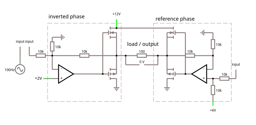
The reference phase part on the right is pretty simple: the op-amp both lifts the input voltage to 6V (the voltage divider at the + op-amp input) and amplifies the signal x2 (the voltage divider at the op-amp – input).
The inverted phase part on the left is just as simple: it, again, re-bases the input voltage, amplifies the signal and inverts the phase.
Caveats: this circuit was designed and ran only in a simulator – I haven’t built and tested it. The input impedance is rather low; if the input signal is weak, an input driver might be required. Alternatively, maybe increasing the voltage divider resistors from 10KΩ to a larger value might increase input impedance, but might introduce noise or other distortions. The circuit liberally uses reference voltages (eg. 2V, 6V) which are a fraction of the operating voltage 12V. I haven’t provided voltage dividers that would derive them from a variable operating voltage, though given the rather large values of the voltage divider resistors, deriving these reference voltages shouldn’t be too hard.
As always, you can play with the circuit at the excellent lushprojects.com [CIR]
Resources
[DPP] Double push-pull amplifier with cross over compensation
https://blog.georgovassilis.com/2021/07/31/double-push-pull-amplifier-with-cross-over-compensation/
[PPA] Push pull output
https://en.wikipedia.org/wiki/Push%E2%80%93pull_output
