update January 2018: there’s a follow-up.
In this off-topic post I’m picking up an old hobby of mine: electronics. I’ve built in the past quite a few analogue audio amplifiers, mostly based on pull-push [1] designs, but always wanted to build a pulsed/switching amplifier. Thus, for no good reason at all, in this post I’ll describe the design I came up with. The awesome and intuitive circuitjs [2] electronic circuit simulator hosted by lushprojects [3] was used for all screenshots and experiments.
If you are impatient for the results, just run the simulation [5].
About audio amplifiers
Audio amplifiers should not distort their signal, otherwise their output would contain audible noise artefacts. Good amplifiers offer near-linear amplification at low powers and low energy efficiency, because their transistors (or vacuum tubes) operate as A-class amplifiers. Their transistors constantly conduct high currents which gives them their linear behaviour at a high energy consumption and low efficiency. I very much recommend the Wikipedia article [4] on the topic.
Switching amplifiers create a burst of rectangular signals which coalesce due to the consumer’s impedance and capacitance into an analogue signal. Transistors are good at conducting either not at all or fully with low energy losses in both states, one has “just” to find a way of generating the right input pulses for the transistors.
Essentially, a switched amplifier consists of a low power pre-amplifier which provides a high input resistance and scales the input signal’s voltage and current to a level suitable for the end stage. Since the pre-amplifier consumes little power it’s OK if its efficiency is low; the entire amplifier’s efficiency is defined mostly be the end stage’s efficiency which consumes most of the power.
Here I’ll focus on the final power amplification stage which drives large consumers. A major assumption is that the input signal has already been pre-amplified to the voltage required by the final stage which adds the current required by the consumer.
Properties of a good amplifier
My ideal audio amplifier would have these properties:
Low distortion: the output signal should be similar to the input signal which means that at the same point in time two samples of the input and output signals should have values close to each other. The amplifier should not increase or decrease the signal’s voltage, nor add noise or change the signal’s phase significantly.
High efficiency: the amplifier should have a high power efficiency converting most of the energy it consumes to the output signal and not to noise nor heat.
High input resistance: the amplifier should not draw much current from the input signal’s source nor feed back into it.
Low output resistance: the amplifier should be able to generate a strong output signal with large currents at the same voltage amplitude of the input signal.
Low complexity: the amplifier’s circuit should be simple.
Stabilise varying output load: the amplifier should be able to adjust to a changing consumer resistance making it suitable for use as an adjustable voltage source.
Everything is configurable: the circuit should achieve any desirable levels for the requirements given above by tuning its configuration.
Operational stability: the amplifier should produce good results when the input power fluctuates, the operation temperature changes or the circuit’s part age.
All of the above requirements are relative: for every quantifiable property P there should be an ideal value Vp of said property and an actually achieved value Vp’ of the implementation so that |Vp-Vp’|<Bp. If the inequality holds for property P then we’ll say that the implementation meets the requirement for that property. E.g. if the maximum permissible phase difference between the input signal and the output signal is 3°, the input signal has a phase of 0° and the output signal has a phase of 2° then the inequality becomes |0-2| = 2 < 3 and the amplifier meets the requirement of phase distortion.
Disclaimer: I’m not claiming that the design described here meets all of these requirements equally well…
First iteration: high-level concept
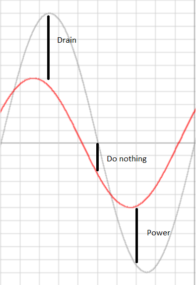
The basic idea is that the amplifier should compare the input voltage to its output voltage and adjust the output voltage when it differs more than a configurable voltage amount. It consists of three components: a comparator which compares the input signal to the output signal, a decision maker that decides how the output signal needs to be modified to approximate the input signal and the end stage which executes the decision maker’s decision.

The comparator (left triangle) is a sensitive, low power component which compares the input signal to the output signal, resulting in a binary “high” or “low” output voltage. More specifically, its binary output means that:
high: the input voltage is higher than the output voltage. The output voltage should be increased to catch up with the input voltage.
low: the input voltage is lower than the output voltage. The output voltage should be decreased to drop to the input voltage’s level.
The decision maker (middle triangle) is a low power component which takes the comparator’s findings and makes a decision about how the output needs to be modified:
high: the output needs more power
low: the output needs to be drained
If it’s input is “high” then the decision maker issues an “add power” command to the end stage which will increase output voltage. If it’s input is “low” then it issue a “drain power” command to the end stage which will decrease output voltage.
The end stage consists of two high-power (e.g. MOSFET) transistors which operate in a complementary C (“all or nothing”) mode. One of the two transistors either conducts fully or not at all. The C mode of operation is the most efficient mode in terms of power consumption. A rapid activation and deactivation of these transistors leads to a series of binary, high-power pulses which approximate the desired output signal.
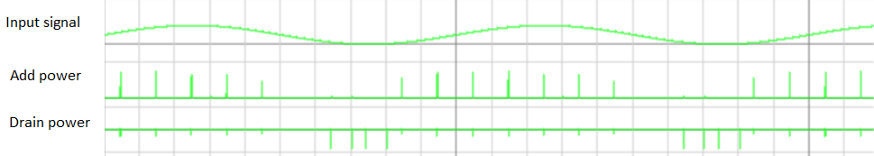
A sample sequence of such “decisions” looks like this:
Second iteration: practical considerations
I’ve brushed some serious considerations under the carpet with the first draft of the design which I’ll try to correct here… by adding more parts to the boxes and triangles of the first design.
The gravest oversight of the first design is that it always activates one of the transistors in the end stage: it either powers the output or drains power from it which would lead to a wildly oscillating output signal, failing the requirements of low distortion and high efficiency. The decision maker so far can issue two commands to the end stage; “power” and “drain”; the command set needs to be extended with a third “do nothing” command:
The decision maker defaults to the “do nothing” command when the output voltage is “close enough” to the input voltage. The definition of “close enough” is configurable and depends on the comparator’s sensitivity. A refined design should take this into account and power or drain the output only if the output signal deviates more than “close enough” from the input signal. The schematic below uses two comparators which respectively assume two distinct responsibilities: the upper comparator produces a “high” output signal only if the input voltage is greater or equal to the output voltage while the lower comparator produces a “high” output signal only if the output voltage is greater or equal to the input voltage. The decision maker is made up of a simple logic circuit which converts the comparator’s output to commands for the end stage.

The end stage commands follow from a simple logical decision table:
| Upper comparator | Lower comparator | Command |
| Low | Low | Do nothing |
| High | Low | Add power |
| Low | High | Drain power |
| High | High | Do nothing |
Third iteration: about comparators
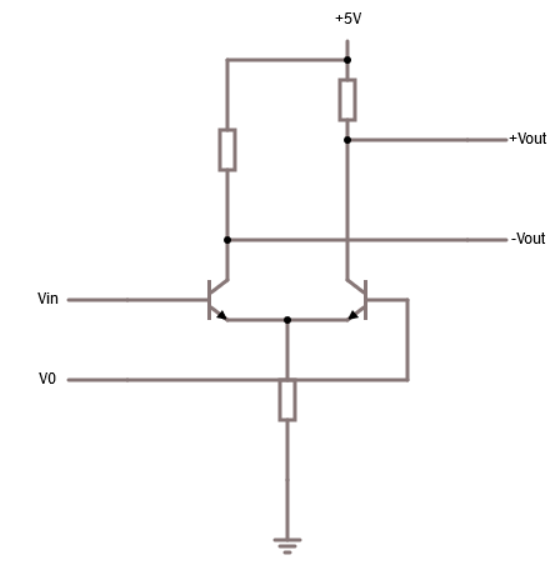
Building a comparator which produces a binary output isn’t that easy. As a matter of fact, I utterly failed to come up with a simple comparator design which can compare two arbitrary input voltages and produce a “yes/no” output. Just like the first two iterations, people take operational amplifiers for granted, but the devil lies in the details: many opamps have complicated circuit diagrams and may require negative voltages. The last observation follows from the schematic of the base differential amplifier. While the input voltage Vin can be measured against the electrical ground potential, the output voltage is the difference between +Vout and -Vout and can not be measured against ground. Translating the output voltage difference to a single voltage against ground seems to be a hard task. I couldn’t figure out a way that would work without transformer coils or an optocoupler.
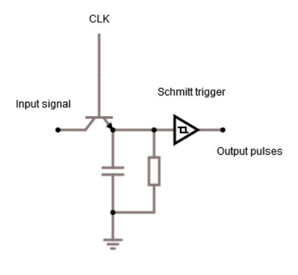
I had to come up with a comparator design which is simple, sensitive and produces a clear “yes/no” decision. The solution settled for is based on the idea that an input signal should briefly charge a capacitor whose discharging time would be a function of the input value thus converting voltage measurement to time measurement.
I’m calling this voltage-to-pulse converter a “sampler”. A clock pulse briefly switches a transistor on and off, connecting the input signal to a capacitor. When the transistor is switched off again the capacitor discharges gradually through a parallel resistor. A (non inverting) Schmitt trigger with a low threshold produces a “high” output as long as the capacitor’s voltage remains above the threshold and produces a “low” output once the capacitor’s voltage drops below that threshold.
The signal diagram below stacks (top-to-bottom) the input signal, the clock pulse, the capacitor voltage and the Schmitt trigger’s output. Note the clear relation between the output pulse duration and the input voltage: longer pulses mean higher input values.

Fourth iteration: final circuit
The circuit depicted below achieves the requirements of a good amplifier to varying degrees. Given that this implementation uses a few tricks and does without complex ICs, I think that the part count speaks for itself. Part values have been picked to lead to good results for low input frequencies (up to 100Hz) which is mainly a limitation of how fast my computer can run the circuitjs simulations. Simulations of higher input signal frequencies would require a higher time resolutions.

For clarity’s sake only the interesting components in the circuit diagram above have been labelled.
The circuit has a distinct symmetry: an upper and a lower “lane” of parts handle the input and output signals respectively. T1,C1,R1 and ST1 make up the sampler for the output signal and T2, C2, R2 and ST2 make up the sampler for the input signal. Since both samplers are driven by the same input clock, their outputs can directly feed the decision maker.
The decision maker consists of two inverters G1 and G2 and the logical AND gates G3 and G4. If, e.g. the upper sampler responsible for the input signal produces a “low” output and the lower sampler responsible for the output signal produces a “high” output, it means that the output voltage is too high and must be drained. In that case G1 inverts the upper sampler’s “low” to a “high” and the G3 produces a “high” output (together with the “high” coming from the lower sampler). T3 is activated and drains the output signal.
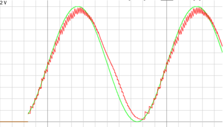
Here is the graph for a 2V input signal (green) and the generated output signal (red):
Considerations
Does it work? The described design fares well in the simulator, but I have not built it and thus can’t say whether it would work if built. [update 03.04.2018] on second thought, it would probably not work; on third thought it might work (see “operational stability” below).
Feedback oscillation came up often while refining the design. Feedback oscillation is caused by overcompensation of the amplifier to changes in the output voltage. If, e.g. the comparator detects that the output voltage is slightly below nominal values and the decision maker decides that the output voltage needs to be reinforced, depending on the sizing of the end stage it is quite possible that the end stage dumps a surge of current on the output, leading to a large increase in voltage. This would subsequently be noticed by the comparator, causing the decision maker to hastily drain the output again eventually leading to oscillation. The design suppresses oscillation through “appropriately” sized L1 and C3 which will soften both powering and draining pulses from the end stage. Although I can’t prove it, I suspect that regardless of the parametrisation of L1 and C3, there will always exist an input signal which tricks the amplifier into oscillation.
Sensitivity is an issue which comes in several flavours. The design assumes a sufficiently pre-amplified input signal which can drive the comparator. Pre-amplification can be achieved with low-power class A transistor amplifiers. Luckily the output signal won’t require pre-amplification because it, obviously, is strong enough to drive anything. Sensitivity of the sampler is very important when generating the pulses which drive the decision maker. The Schmitt triggers must have a “low” threshold, otherwise low input signals won’t trigger any pulses. The design discussed here assumes a 1:1 voltage amplification, but if the input amplitude is too low to trigger the sampler, then a low-power voltage amplifier can be used in front of either the transistor switches or the Schmitt trigger. Luckily those pre-amplifiers don’t need to be linear as long as their behaviour is identical for both samplers: any distortion introduced by the pre-amplifiers equally affects both samplers and will be compensated by the decision makers. Last not least, the clock signal which drives the samplers in combination with the RC pair is kind of important. If it is too fast then the capacitors will neither fully charge nor discharge, limiting the input range for the Schmitt triggers and thus limiting the range of pulse durations that drive the decision makers. This means that the decision makers will “see” the comparators in mostly an undecided state and decide to do nothing, thus neither powering nor draining the output. If the clock signal is too slow then the samplers would adjust slowly to changes in both the input and the output signal, causing the decision makers to not react quickly enough to fluctuations.
Conceptually speaking, there seems to be a tradeoff between sensitivity and reaction time to changes. A configuration which is sensitive and picks up small differences between the input and output signal produces accurate commands to the end stage, but at a low rate. A configuration which reacts faster to changes in the input or output signals tends to “overcompensate” and oscillate. I suspect an underlying effect similar to quantum physics’ uncertainty principle.
Efficiency is another big topic. Measuring efficiency requires a better engineering background than I have, so I relied on circuitjs’ measurements… which, unfortunately don’t seem to work well with AC. So I’ll rest on the argument that all circuit parts except the end stages are low-powered transistor designs which consume little power. The amplifier’s efficiency is mostly defined by what goes on in the end stages. Since the end stages operate in the efficient C mode, efficiency must be better than any class A or class B amplifier.
Distortion: the design produces a significant amplitude and phase distortion visible in both the “ripples” of the red wave and a distinct “lagging” of the red wave behind the green wave. The “ripples” are caused by the reaction time of the samplers and can be reduced by increasing the sampler clock frequency (with all the pros and cons discussed earlier). The ripples can also be decreased by increasing the LC values, but that would decrease output power (see below). The “lag” between input and output can partially be reduced by increasing the sample frequency, but it’s important to not mistake low sensitivity for lag. E.g. the output signal shown below never reaches down to 0V although the input signal does, which makes it look like the output signal is lagging behind the input signal for low values:
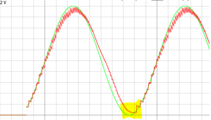
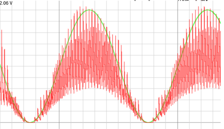
Significant distortion is also caused by high output load. E.g. below is the output for the same circuit with a 2Ω output resistance. The strong ripples in the output signal are clearly visible as the end stage struggles to provide enough power.
Bandwidth is another topic akin to sensitivity and distortion. The design presented is capable of handling very low frequencies, including 0Hz, which makes it a suitable variable voltage source. The amplifier might be suitable for higher frequencies as long as the sampler can cope with them; the sample clock’s frequency must be significantly higher than any frequency in the input signal and the end stages must be powerful enough to power or drain consumers quickly enough. Especially the latter might require lower values for the output coil in order to not limit currents too much which, in turn, might lead to oscillation through overcompensation.
Operational stability is something I didn’t touch with the design. For one, because circuitjs doesn’t simulate the effects of temperature on (ageing) parts. [update 04.03.2018] Simulating ageing parts is possible by just changing their values. Doing so (eg. lowering C1) quickly reveals that the analogue circuit components are sensitive to changes in their values and the output signal quickly diverges significantly from the input signal. I didn’t come up with a self-correcting mechanism (I suspect that would require significant expansion of the design’s digital portion) but there’s a simple manual fix: connecting ST1 (or ST2) to a potentiometer and tuning the potentiometer fixes almost any issues with part tolerances in the analogue part of the circuit. This is because the potentiometer changes the Schmitt trigger’s threshold, modifying the sampler’s pulse length.
Fluctuations in operation voltage may not be that important after all; the “pre” parts of the circuit (sampler, decision maker) can be shielded from voltage fluctuations with a simple voltage stabilizer since their power consumption is low. The end stage will be affected by voltage fluctuations, but the entire point of this design is to compensate fluctuations in the output signal. As long as the operational voltage doesn’t drop too low for too long, the amplifier should be able to compensate unstable op voltage. Just for the fun of it, I replaced the op voltage in the simulation with a 5V 100Hz signal (see below). The results are not pretty, but not too bad either. The op voltage dip can be seen clearly as the output signal (red wave) drops with it, but the moment the op voltage rises again, the output wave follows suit, not overcompensating for the time lost but dropping together with the input signal.

Output power: the current design doesn’t produce high output powers. The input signal’s amplitude is 2V which isn’t suited for high power outputs, unless the consumer’s resistance drops well below 1Ω. You can play with the part parameters and see what happens: e.g. decreasing R5 to some mΩ will greatly increase the consumed power, but the output signal’s amplitude will be limited. The amplitude can be boosted by increasing transistor performance (increase beta/hFE) and reducing L1, which in turn will increase ripples. In order to keep those at bay, you’ll need to increase C3. Rinse and repeat, you should get there.
While playing with the circuit configuration may lead to results in theory, it will be hard to actually obtain output loads in the milli-ohm range or super-buff end-stage transistors. In reality, high output powers will require voltage amplification which means that although the input signal has a 2V amplitude, the output signal will require a 40V amplitude, abandoning the “no distortion” premise (a multiplied output amplitude is a severe distortion).
A far more fundamental limitation is the way the amplifier deals with higher voltages. Let’s assume two samples Vin and Vout of the input and output signals at the same time. Let’s assume that both have already high values but Vout < Vin. The decision maker decides that the output voltage has to increase. The problem here is that the samplers responsible for the input and output signal will produce two long pulses Pin and Pout with Pout < Pin; the, rather short, difference between the pulses ΔP = Pin – Pout just isn’t long enough to drive the end stage to produce sufficient power in order to get Vout up to Vin. Remember that since Vin and Vout are “large”, Pin and Pout will be long pulses, so the decision maker decides for most of the time to “do nothing”. There’s a fundamental problem with physics here: because the power consumed on a resistance R under voltage V is RV², it takes much less energy to go from e.g. 1V to 2V (R2² – R1² = 3R Watt) than to go from 3V to 4V (R4²-R3² = 7R Watt). This issue could possibly be compensated with a non-linear pre-amplifier which would lead to disproportionately longer sampler output pulses for higher signal values, but I have not tested that.
One last topic I didn’t look into, at all, is RFI (radio frequency interference) issues which is a major issue for amplifiers and especially switched amplifiers which operate at high powers and frequencies.
References
[1] Pull-push amplifier
https://en.wikipedia.org/wiki/Push%E2%80%93pull_output
[2] Circuitjs
https://github.com/sharpie7/circuitjs1
[3] Lush projects
http://lushprojects.com/circuitjs/circuitjs.html
[4] Amplifiers
https://en.wikipedia.org/wiki/Amplifier
$ 13 0.000001 13.097415321081861 50 5 43
R 48 64 0 64 0 1 50 1 1 0 0.5
r 496 224 720 224 0 12000
r 784 224 784 352 0 50
w 144 352 144 224 0
R 656 16 688 16 0 0 40 5 0 0 0.5
c 224 64 224 208 0 1e-8 0.3265284859465699
t 176 112 176 64 1 1 0.5125079275550852 0.5372834728163942 100
r 176 208 176 112 0 100000
w 288 64 224 64 0
r 288 64 288 208 0 6000
182 288 64 368 64 0 1.5 0.12 0.12
182 288 352 368 352 0 1.5 0.12 0.12
r 288 352 288 208 0 6000
w 288 352 224 352 0
r 176 304 176 208 0 100000
t 176 304 176 352 1 1 0.5121001932310978 0.539825885259068 100
w 192 352 224 352 0
c 224 208 224 352 0 1e-8 -0.3761830296382112
r 48 64 160 64 0 10000
w 224 64 192 64 0
w 224 208 288 208 0
g 288 208 336 208 0
150 448 80 544 80 0 2 0 5
I 368 96 448 96 0 0.5 5
c 720 352 720 224 0 0.00009999999999999999 -0.8424786416363813
150 448 336 544 336 0 2 0 5
I 384 320 448 320 0 0.5 5
t 608 336 656 336 0 1 -1.16110415799115 1.0116110415785067e-11 300
g 784 352 784 384 0
r 608 336 544 336 0 100
w 368 96 368 352 0
w 384 320 384 64 0
w 720 224 784 224 0
w 656 320 656 160 0
l 720 224 720 160 0 0.000009999999999999999 2.026365186758028e-13
207 48 64 48 112 0 Input
207 784 224 848 224 0 Output
207 48 208 48 160 0 Sampling clock
t 608 80 656 80 0 1 -4.99999999998934 -1.1611041579906167 300
x 484 338 500 341 4 12 G3
x 406 297 422 300 4 12 G1
x 661 338 675 341 4 12 T3
x 669 89 683 92 4 12 T4
x 165 47 179 50 4 12 T2
x 173 363 187 366 4 12 T1
w 48 208 176 208 0
r 544 80 608 80 0 100
207 656 64 704 64 0 Vop
w 656 96 656 160 0
w 448 64 384 64 0
w 368 352 448 352 0
w 720 352 656 352 0
w 784 352 720 352 0
R 48 208 16 208 1 2 4000 2.5 2.5 0 0.4
x 239 302 255 305 4 12 C1
x 239 158 255 161 4 12 C2
x 300 300 316 303 4 12 R1
x 298 164 314 167 4 12 R2
x 323 333 345 336 4 12 ST1
x 315 95 337 98 4 12 ST2
x 486 87 502 90 4 12 G4
x 398 126 414 129 4 12 G2
x 689 201 703 204 4 12 L1
x 682 290 698 293 4 12 C3
x 569 105 585 108 4 12 R4
x 569 305 585 308 4 12 R3
x 798 277 814 280 4 12 R5
r 656 16 656 64 0 0.1
w 384 64 368 64 0
w 160 352 144 352 0
w 496 224 144 224 0
w 720 160 656 160 0
o 35 64 0 12290 2 0.0001 0 2 36 0
