Last year I wrote about A switching amplifier electronic design which can drive large power loads with high efficiency and tolerable distortion. The operational principle for this is that a pre-stage converts the input signal into a series of pulses which rapidly switch the end-stage on and off – that is a power-efficient mode of operating transistors under large loads. The circuit suffered from a major limitation, namely the pulses were narrow, switching the end-stage transistors on only for a short time. The old design required massively over-provisioned transistors and generates large current spikes.
I’d like to talk about a slightly improved design which produces longer pulses, driving the end-stage transistors for a longer time and thus smoothening current spikes.
The parts have been dimensioned to handle low frequencies from 0 Hz to about 100 Hz, but that’s just a limitation of the simulator I used for designing the circuit – there’s nothing keeping you from lowering the capacitors’ values and increasing the clock rate to deal with a broader input signal bandwidth.
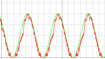
Green: input signal. Red: output signal 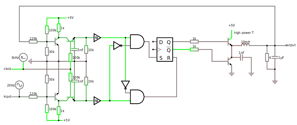
circuit diagram
First the “big picture”: the amplifier compares the input signal to its own output signal; when the output signal voltage is lower than the input signal voltage, the amplifier drives more power to the output. If the output signal is larger than the input signal, the amplifier drains power from the output.
Pre-amplification stage
First, the new design has a pre-amplification stage in the common emitter configuration. The input resistance is 120K which is large enough to not disturb the input signal. This stage has a high amplification, but introduces distortion and inverts the signal. Now, it turns out those two drawbacks aren’t that bad after all, because the circuit works like a differential amplifier: as long as the same distortion happens to both branches of the amplifier, they cancel each other out.
Sampling stage
The next stage converts the analogue input signal into a series of pulses by quickly charging and discharging capacitors and measuring their discharge time. A Schmitt trigger converts the capacitor discharge curves into pulses. Sizing capacitors is crucial here: too high values will lead to “smudged” discharge curves with a low amplitude when one spike fades into the next, making it hard for the trigger to distinguish them. Too low values will lead to thin discharge curves which just look all alike.
A low trigger threshold is desirable, as it essentially constitutes the amplifier’s sensitivity. The voltage threshold in this circuit is 0,2V; higher thresholds will make it impossible to pick up lower input signal amplitudes. If, for practical reasons, it is not possible to configure such a low threshold, then the preamp stage should amplify the signal which would distort it and cramp it towards the higher end. Again, because of the differential nature of the amplifier, the distortion in both branches would cancel each other out, but there would be a loss in sensitivity in higher signal values.
Comparator stage
The next stage is just a couple of AND gates which compare the pulses from both branches of the amplifier and generate commands for the power stage. The upper branch produces a logical 1 when the output signal needs more power, the lower branch produces a logical 1 when the output signal needs to be drained. The old amplifier design directly drove the power stage with those two commands. The issue here is that the comparator stage issues most of the time 0 for both branches, because the sampling stage needs a full clock cycle to compare the input signal to the output signal and issues the sampling result shortly at the end of a sampling cycle. These short pulses are not long enough to drive sufficient power in the power stage. The new design remembers the command in a flip flop, thus generating a clear “more power” or “less power” command for the full duration of a cycle.
Power stage
The power stage consists of two powerful transistors which operate as C-class amplifiers: they either conduct fully or not at all, corresponding to the commands generated in the comparator stage. This mode of operation is power efficient, but requires a fast sequence of output pulses and a bit current smoothening in the form of a small coil and capacitors.
Discussion
Most issues have been discussed in the previous post, so here I’d like to talk about a few considerations omitted earlier. The purpose of this circuit is to drive large power loads with high efficiency and minimum distortion. The distortion can be arbitrarily reduced by increasing the sample rate. The circuit, however, does not perform well with light loads as it tends to oscillate. When the output load is low ( = high resistance), any output command will result in a large voltage change, which will cause the comparator to issue the opposite command -> oscillation. The previous circuit did better, because it could issue a “hold” command which didn’t modify the output signal at all as long as it didn’t diverge more than a threshold from the input signal.
