From the producer of A switching amplifier [AM1], A better switching amplifier [AM2] comes part 3: An even better switching amplifier. A quick recap: we’re looking into class D switching amplifiers for their high efficiency and power output. The first amplifier sampled the input signal by taking voltage snapshots with a capacitor and measuring the discharge time which produced a PWM signal that drove the final stage. The second amplifier improved output power and efficiency by producing wider PWM signals. This third circuit is a re-design which replaces the store & hold capacitor sampling stage with voltage comparators and a flip-flop. As always, there is a circuit.js simulation [CIR] of this design to play with.

Design overview
Just like the other two, this is a feedback amplifier which compensates deviations between output and input, trying to minimise differences between output and input. The output impedance is low so that high loads can be driven. The input signal (here, a 50 Hz sine wave) is balanced around 0V which means that there is no DC current. Rload is an output resistor which represents the workload (eg. a speaker) which we’d like to supply with power.
The amplifier supplies an output signal to the load resistor which is balanced at an arbitrary offset voltage so that a symmetrical AC voltage drives AC current through the load. This is an important improvement over the previous amplifiers which used output capacitors to block DC current from leaking into the load, with the unintended side effect being that it behaved like a high-pass filter. Now, since we’re not using capacitors any more, very low frequencies can be amplified (yay boom boxes!) and the amplifier doesn’t filter out frequencies any more. The tiny coils are just there to block spikes from the switching transistors – the lower Rload is, the smaller these coils can be made, so to let high frequencies through.
OP1 is configured as a differential voltage amplifier and outputs the difference between 0V and the signal… which in this example, coincidentally is always equal to the input signal, but the principle matters. OP2 has the same function, but computes the voltage difference on Rload. If the voltage driving Rload was balanced around 0V we wouldn’t need OP2, but generally speaking the voltage bias is unknown. Both OP1 and OP2’s output are raised by the expected input signal amplitude, hence 1V, so that they don’t output negative voltages; experiments with various reference voltages from 1V to half the operating voltage (here: 2.5V) showed no further effect on the output signal, so it’s probably easier to obtain a reference voltage through a voltage divider from the operating voltage. OP3 compares OP1 and OP2’s output and outputs 0V or 5V which tells us whether the input signal is larger or smaller than the output signal; that’s the compensating feedback loop. In the first case the amplifier needs to supply more top-down current (T1->T2), in the latter case it needs to supply more bottom-up (T4->T3) current.
We could feed OP3’s decision directly to the driver stage (T1, T2, T3, T4), but that would create a direct feedback loop which would oscillate at a very high frequency, introduce distortion and trash the circuit’s efficiency. Instead, the circuit uses a D flip-flop which samples OP3’s decisions at a specified clock frequency (here: 100 kHz) and drive the output stage accordingly. The flip-flop produces stable pulses for the output stage which is key to both high output power and efficiency.
The output stage consists of four MOSFET transistors (T1, T2, T3, T4) in a full-bridge configuration. When the upper part of the bridge conducts, current flows from T1 through the load to T2. When the lower part of the bridge conducts, current flows in the opposite direction from T4 to T3.
Notes & caveats
Just a simulation: as all other circuits discussed previously, this circuit exists only in the simulator, was not built and not tested. For all that matters, it might not work in reality.
Negative voltages: OP1 and OP2 output negative voltages up to the amplitude of the input signal. This is an annoying limitation of the current design that might be rectified in a later version. [2025.08.28] The new design rises OP1 and OP2’s comparison voltage to 1V which eliminates negative voltages. The comparison voltage should be the expected maximum input signal amplitude.
MOSFET drivers: it’s silently assumed that the flip-flop is capable of driving the end stage which operates at 5V. Should the end stage operate at higher voltages and switching frequencies, extra drivers might be required.
Sampling frequency: In theory, higher sampling frequencies lead to cleaner outputs. The 100 KHz sampling frequency in this design is a semi-arbitrary choice; the output signal looks clean to the eye, higher frequencies slow the simulator down. Very high sampling frequencies would distort digital signals and drive the MOSFETs with unclean timing, which would reduce power and efficiency.
[2025.08.28] Input resistors: there are various input resistors arbitrarily chosen at 100KΩ. The point is to avoid drawing too much current from input signals so as not to distort them, but still provide enough current for the amplifiers to function and “short” interference signals. A real circuit would probably require some experimentation to get the values right.
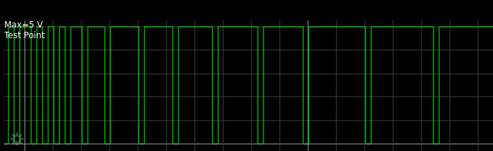
[2025.08.28] PWM: the digital signal driving the power stage merits some investigation. D-class amplifiers usually drive the end stage with pulses whose width varies with the intended output power: the more power the end stage is to produce, the wider the pulses. By looking at this circuit’s diagram, one would deduce that all pulses have the same width, namely that of the clock’s duty cycle. However that is not the case; the feedback loop actually may cause clock cycles to coalesce into wider pulses, as the graph of OP3’s output shows:
Resources
[AM1] A switching amplifier
https://blog.georgovassilis.com/2018/03/03/a-switching-amplifier/
[AM2] A better switching amplifier
https://blog.georgovassilis.com/2019/01/12/a-better-switching-amplifier/
